Through Glass Via (TGV) Technology: Precision Micro-hole Machining Solution
Solutions News · 2026/9/30 · 2 views
Micro-hole forming for vertical electrical interconnection of glass substrates (Through Glass Via, TGV) in advanced packaging, high-density interconnection (HDI) 3D stacking, RF module and MEMS packaging. The equipment is capable of fabricating hole structures with a minimum aperture of 5–20μm and an aspect ratio of 50:1, featuring smooth hole walls with a roughness Ra < 0.2μm, and provides low-loss interconnection paths for 3D chip interconnection.
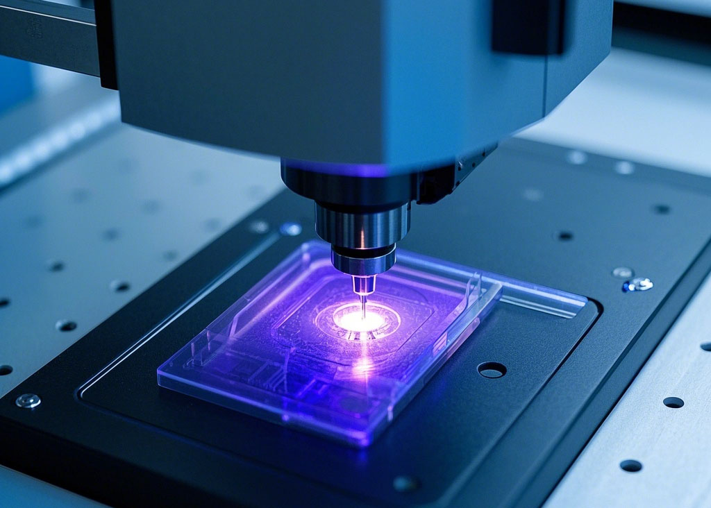
As Moore's Law gradually approaches its physical limit, advanced packaging technology is placed with high expectations. Among numerous technical routes, Through-Glass Via (TGV) technology, with its unique material advantages and process potential, is emerging as a key force reshaping the chip interconnection landscape. However, one of the core bottlenecks for the large-scale industrialization of TGV technology lies in the precision micro-hole forming process. The ability to realize high-precision, high-aspect-ratio, and high-consistency via processing on glass substrates is an important reflection of equipment and process capabilities. This article will discuss solutions for TGV precision micro-hole processing by combining industry trends and process practices.
Ⅰ. Why TGV Attracts Extensive Attention?
Traditional Through-Silicon Via (TSV) technology has laid the foundation for 3D packaging, but the high-frequency loss, manufacturing cost, and process complexity of silicon materials limit its application in certain scenarios. Glass substrates, with their unique physical properties, provide a better solution for advanced packaging.
1.Low dielectric loss: The dielectric constant (approximately 4-5) and loss factor of glass are much lower than those of silicon, which means that TGV can significantly reduce signal attenuation and delay in high-frequency signal transmission, showing obvious advantages especially in high-frequency applications such as 5G/6G radio frequency frontends and millimeter-wave radars.
2.Large-size and ultra-thin capability: The manufacturing process of glass panels is mature, enabling cost-effective production of large-size (e.g., 510mm×515mm) ultra-thin substrates (thickness can be less than 100μm), which effectively alleviates the warpage problem in large-size packaging and improves packaging yield.
3.Insulation performance: Glass is a natural insulator, eliminating the need for additional deposition of an insulating layer on the inner wall of vias as required for silicon substrates. This simplifies the process, reduces costs, and avoids the risk of thermal mismatch between the insulating layer and the substrate.
4.Adjustable coefficient of thermal expansion (CTE): By adjusting the glass formula, its CTE can be matched with silicon chips or other packaging materials, reducing the risk of stress failure during thermal cycling.
ⅡTGV Micro-hole Forming: Core Process Difficulties
The manufacturing process of TGV mainly includes three links: laser drilling, wet etching for hole expansion, and metallization filling. Among them, laser drilling is the first process that determines the uniformity of subsequent hole expansion and metallization quality, and it is also the link with the most concentrated technical difficulties.
The material properties of glass substrates pose many challenges to their micro-hole processing. First, glass has high hardness but low toughness, making it extremely prone to edge chipping and microcracks in traditional mechanical processing. Second, glass has low thermal conductivity. If the laser pulse width is too long or the energy is too high, heat accumulates inside the material, which easily leads to thermal stress cracks and excessive hole wall roughness. Third, when the aperture is reduced to below 20μm and the aspect ratio exceeds 10:1, the laser focus needs to be accurately positioned at a specific depth inside the glass, which puts forward higher requirements for beam quality and focus control.
The core evaluation indicators of TGV technology mainly include aperture accuracy, aspect ratio, hole wall roughness, edge chipping size, and heat-affected zone. Among them, the aspect ratio directly affects the process window of subsequent metallization hole filling, while the hole wall roughness determines the bonding force between the metal layer and glass and signal integrity.
Ⅲ、TGV Micro-hole Processing Solution from JiajiaYong Laser
Shenzhen JiajiaYong Laser Equipment Co., Ltd., relying on the technical guidance of the Laser Optics Research Institute of the Chinese Academy of Sciences, has developed a dedicated laser micro-hole processing platform for glass via applications, forming a process solution that balances accuracy and efficiency in the TGV drilling process.
1.High-precision micro-hole forming capability: By optimizing the Bessel beam shaping system, JiajiaYong Laser's equipment can realize micro-hole processing with an aperture as low as 5–20μm on a 1mm-thick glass substrate, with an aspect ratio exceeding 50:1. Through precise control of laser energy and focus position, the hole wall roughness can be controlled at Ra < 0.2μm, and the orifice edge chipping size can be controlled within a small range, creating favorable conditions for subsequent wet etching hole expansion and metallization filling.
2.Cold processing process guarantee: In view of the low thermal conductivity of glass materials, JiajiaYong Laser adopts picosecond/femtosecond ultrafast laser light sources. With an extremely short pulse width (10⁻¹² second level), material removal is completed before heat diffusion occurs, and the heat-affected zone can be controlled within 1μm. This processing method fundamentally reduces the probability of thermal stress cracks and ensures the mechanical integrity of the via array.
3.CCD visual positioning and compensation: Glass substrates are prone to minor deformation due to stress release during processing, which affects the position accuracy of the via array. JiajiaYong Laser's equipment integrates a high-precision CCD visual positioning system, which can automatically identify the alignment marks on the substrate before processing, complete expansion and contraction compensation and position correction, and ensure the position accuracy of thousands of vias on large-size panels.
4.Industrial-oriented batch processing capability: The equipment is equipped with a high-precision motion platform and an automated loading and unloading system, supporting the whole process of processing from sample trial production to batch production. The equipment can adapt to glass substrates of different thicknesses (0.1mm–2mm) and different sizes, meeting the TGV micro-hole processing requirements from R&D verification to mass production ramp-up stages.
Ⅳ、Industrial Application and Prospect
TGV technology is moving from the laboratory to industrialization. According to market research机构 forecasts, the global TGV packaging market size is expected to reach hundreds of millions of US dollars in 2026, maintaining a high compound annual growth rate.
On the application side, TGV technology has shown clear implementation paths in multiple fields:
1.AI computing chips and high-performance computing: The high flatness and low warpage characteristics of glass substrates make them a strong candidate for large-size, multi-chip system-in-package, providing low-loss interconnection substrates for heterogeneous integration.
2.Radio frequency front-end modules (RF FEM): Low dielectric loss provides high-quality signal transmission channels for 5G/6G millimeter-wave frequency bands, effectively reducing insertion loss.
3.MEMS and sensor packaging: The CTE matching characteristic between glass and silicon makes it an ideal packaging substrate for MEMS inertial sensors, pressure sensors and other devices.
4.Optical communication and photonic integration: The low absorption characteristic of glass in the near-infrared band supports the hybrid integration of optical waveguides and electrical interconnections.
Ⅴ、Conclusion
The progress of TGV technology is not only related to the forming accuracy of a single micro-hole, but also related to whether the advanced packaging industry can carry the computing power demand of next-generation chips with lower cost and higher reliability.
JiajiaYong Laser continues to deepen its efforts in the field of glass via micro-hole processing, and is committed to promoting the industrialization process of TGV technology with precision micro-hole forming processes.
If you have technical needs in the field of glass via micro-hole processing or advanced packaging, welcome to communicate with JiajiaYong Laser's technical team to obtain program evaluation and sample testing support tailored to your substrate materials and process requirements.